DE10-Nano signal reference
This page describes the board-facing signals in the released 32-bit DE10-Nano design. The assignments in pulsepins.sv and pulsepins.qsf are authoritative; use the Terasic DE10-Nano documentation for physical header pin numbers and board-level electrical limits.
Electrical baseline and output enable
The released design uses 3.3 V LVTTL signaling on its PulsePins-facing GPIO and Arduino-header signals.
The 32 main qout pins use bidirectional FPGA buffers. They default to high impedance while physical output enable oe is low, allowing the readback and counter paths to sample externally driven levels. The same oe also controls the bidirectional streamer_qout_valid and streamer_qout_strobe pads. When oe is high, PulsePins drives these signals. Avoid connecting an enabled output to another active driver.
Use high-impedance instrument inputs on unbuffered FPGA pins. Do not apply a direct 50 ohm scope termination unless an external driver or buffer has been designed for that load.
GPIO signal map
The main output and control signals use the two 40-pin DE10-Nano GPIO headers. The image below gives the physical overview.
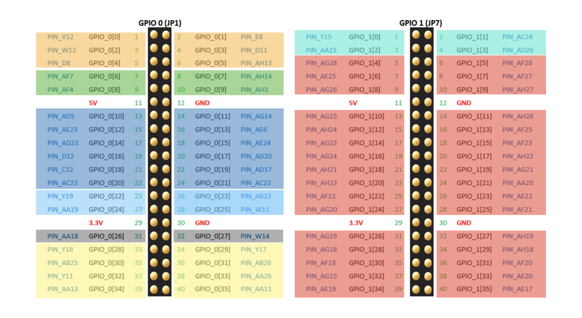
Color code used in the diagram:
| Color | Meaning |
|---|---|
| orange | clocking |
| green | status |
| blue | triggering |
| yellow | AUX I/O |
| cyan | external clock inputs |
| red | output data |
The indexes below are positions in the top-level GPIO arrays, not physical connector pin numbers. GPIO0 bits 22-25 use the current EXTRA_SETB debug selection; an alternate build can expose streamer trigger visibility instead.
Quick connections for the first-output manual chapters:
| Signal | Logical index | DE10-Nano header pin | FPGA pin |
|---|---|---|---|
qout[0] |
GPIO1[4] | GPIO 1 (JP7) pin 5 |
PIN_AG28 |
qout[1] |
GPIO1[5] | GPIO 1 (JP7) pin 6 |
PIN_AF28 |
| ground | - | GPIO 1 (JP7) pin 12 or pin 30 |
- |
Use the numbered connector drawing above to verify orientation before attaching a probe.
| Connector | Index | Debug label | Signal | Function |
|---|---|---|---|---|
| GPIO0 | 0 | D0 | streamer_qout_strobe |
output strobe pulse |
| 1 | D1 | oe |
physical output enable | |
| 2 | D2 | streamer_clk |
selected output clock | |
| 3 | D3 | streamer_qout_valid |
output sample qualifier | |
| 4 | activity |
recent output activity | ||
| 5 | heartbeat |
FPGA image and reference-clock indicator | ||
| 6 | D8 | trigger_armed |
waiting for a trigger event | |
| 7 | D9 | trigger_activated |
triggered and advancing output | |
| 8 | D10 | done |
clean stream completion | |
| 9 | D11 | buffer_error |
output FIFO underrun detected | |
| 10 | ext_trigger_enable |
external trigger enable input | ||
| 11 | ext_trigger_force |
external trigger force input | ||
| 12 | ext_trigger_reset |
external trigger reset input | ||
| 13 | gate_in |
output-advancement gate input | ||
| 21:14 | ext_trigger_in[7:0] |
external trigger inputs | ||
| 22 | D12 | rnd1 |
synthetic random debug output (EXTRA_SETB) |
|
| 23 | D13 | rnd2 |
synthetic random debug output (EXTRA_SETB) |
|
| 24 | D14 | 0 |
constant-low debug output (EXTRA_SETB) |
|
| 25 | D15 | 0 |
constant-low debug output (EXTRA_SETB) |
|
| 26 | I2C SDA | HPS I2C data | ||
| 27 | I2C SCL | HPS I2C clock | ||
| 35:28 | AUX[7:0] |
auxiliary I/O | ||
| GPIO1 | 0 | EXT_CLKp |
external streamer-clock input | |
| 1 | PPS_IN |
pulse-per-second input | ||
| 2 | PPCLK1 |
reserved; unconnected in the released top-level design | ||
| 3 | PPCLK2 |
reserved; unconnected in the released top-level design | ||
| 35:4 | D[7:4] for qout[3:0] |
streamer_qout[31:0] |
main output bus |
Arduino header
The released build also presents selected output and clock signals on the Arduino header for probing and tests:
| Arduino signal | PulsePins signal |
|---|---|
| D0-D7 | streamer_qout[7:0] |
| D8 | streamer_clk |
| D9 | core_clk |
| D10 | int_clk |
| D11 | streamer_qout[0] |
| D12 | streamer_qout[1] |
| D13 | PPS_XTAL |
| D14-D15 | constant low |
These Arduino-header signals are direct output assignments and are not released by oe. Do not drive them from external logic; use high-impedance probes or connect them only to compatible inputs.
On-board LEDs
LED0 is closest to the Ethernet connector. The LEDs are active high and show:
| LED | Signal | Meaning |
|---|---|---|
| 0 | trigger_armed |
waiting for a trigger |
| 1 | trigger_activated |
trigger fired |
| 2 | done |
clean stream completion |
| 3 | buffer_error |
output FIFO underrun |
| 4 | streamer_trigger_in[0] |
combined trigger input 0 |
| 5 | streamer_trigger_in[1] |
combined trigger input 1 |
| 6 | activity |
at least one valid output event was observed in the recent 200 ms window |
| 7 | heartbeat |
FPGA image loaded and reference clock running |
Manual trigger controls
The miscellaneous trigger-combiner input receives these on-board controls:
- KEY0 and KEY1 provide trigger inputs 0 and 1
- switch 0 provides trigger enable
- switch 1 provides trigger force
- switch 2 provides trigger reset
PPS_INprovides miscellaneous trigger input 2
The switches are off when positioned toward the Arduino connector. See the Combiner subsystem for source selection and pptrig for live diagnostics.
Trigger monitor PIO
pio_trig_monitor exposes both the external trigger pins and the post-combiner signals to software.
External signals occupy the low fields:
| Bits | Signal |
|---|---|
| 7:0 | ext_trig_in |
| 8 | ext_trig_enable |
| 9 | ext_trig_force |
| 10 | ext_trig_reset |
Signals seen by the streamer occupy the upper fields:
| Bits | Signal |
|---|---|
| 23:16 | streamer_trig_in |
| 24 | streamer_trig_enable |
| 25 | streamer_trig_force |
| 26 | streamer_trig_reset |
Auxiliary I/O
The released design exposes eight bidirectional AUX pins. Direction is selected independently for each bit through pio_cfg: 0 selects input, 1 selects output, and all bits default to input after reset. pio_aux holds output values and reports sampled pin levels.
ppaux samples the bus but does not configure direction or drive output values. The PP_PMOD hardware reference documents the J12 AUX connector.