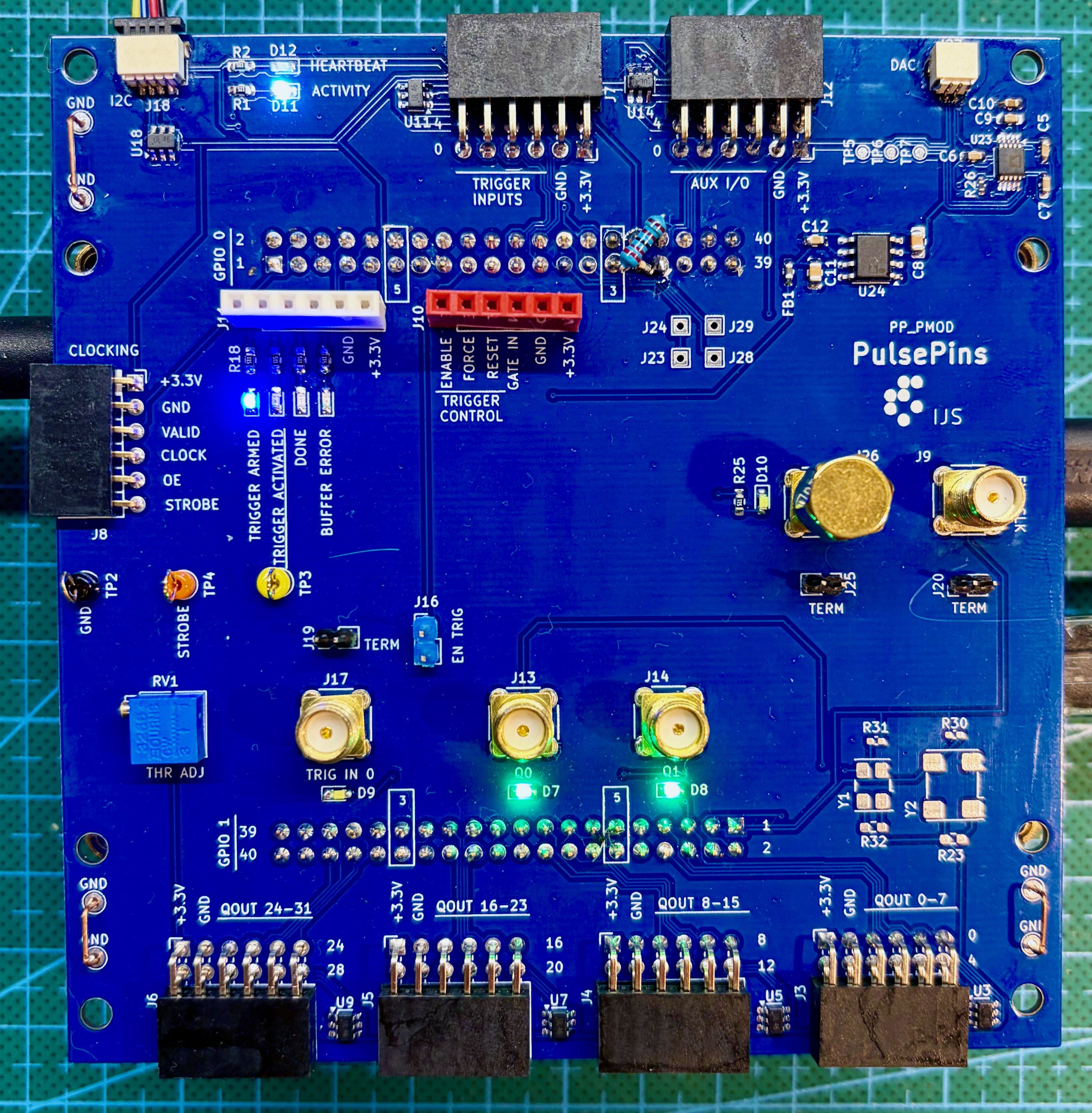
PP_PMOD Reference Shield
PP_PMOD is the reference KiCad shield design for attaching PulsePins to the DE10-Nano GPIO headers and bringing the FPGA I/O out to lab-friendly connectors.
It is an optional hardware profile rather than a required baseline. The board is intended both as a usable shield and as a starting point for derivative designs with different connectors, buffering, or peripheral choices.
Revision and source
The top-level KiCad project is pcb/ppshield_pmod/shield.kicad_sch with title PP_PMOD: GPIO shield for DE10-Nano, revision 1, and date 2025-09-20.
Project files:
- KiCad sources:
pcb/ppshield_pmod/ - Top-level schematic:
shield.kicad_sch - PCB layout:
shield.kicad_pcb
Feature summary
The reference design includes:
- four 8-bit output connector groups carrying
Q0..Q31 - one 8-bit auxiliary connector carrying
AUX0..AUX7 - a trigger-input connector group plus a separate SMA trigger input path
- two buffered SMA outputs for instrument connection
- SMA inputs for
EXT_CLKandPPS_IN - a Qwiic-compatible I2C connector for external modules
- an onboard
MCP9808temperature sensor - an onboard
AD5693DAC with a separate low-noise regulator - status, activity, and heartbeat LEDs
- test points and probe-grounding features
- optional oscillator-module footprints and optional input terminations
The QOUT, AUX, and trigger connector groups use PMOD-style 2x6 mechanics; for the baseline mechanical/electrical convention, see the Pmod Interface Specification.
All of the external connector-facing signal groups in the design are protected with ESD devices.
Board architecture
The KiCad hierarchy is already a good map of the board:
GPIOconnects the shield to the DE10-Nano headersQOUThandles the main 32-bit output bus and related control/status linesoutput buffersdrives the two SMA output channelsTriggeringhandles trigger connectors, trigger control/status, and the thresholded SMA trigger pathext_clkhandlesEXT_CLK,PPS_IN, optional termination, and oscillator-module optionsI2Ccontains the Qwiic connector, onboardMCP9808, and onboardAD5693AUXbrings out the auxiliary busLEDsdrives the board indicatorsMisccontains test points and grounding aids
Optional features
Several parts of the board are optional or configuration-dependent:
- the onboard DAC path is optional
- the onboard temperature sensor is optional
- the oscillator footprints are optional
- some terminations are selectable or optional
- the exact shield assembly may differ from the fully populated schematic
When documenting or validating the board, record which optional parts are populated and which jumper positions are used.
Hardware reference
All board-level connectors, timing inputs, onboard peripherals, jumpers, and test points are documented on PP_PMOD hardware reference.
Connector index
Quick reference for the board's main external interfaces:
| Ref | Purpose |
|---|---|
J3-J6 |
four 8-bit QOUT groups |
J7 |
8-bit trigger input bus |
J8 |
QOUT sideband header |
J9 |
EXT_CLK SMA input |
J10 |
trigger control header |
J11 |
trigger/status header |
J12 |
AUX bus |
J13 |
buffered Q0 SMA output |
J14 |
buffered Q1 SMA output |
J17 |
thresholded trigger SMA input |
J18 |
Qwiic I2C connector |
J26 |
PPS_IN SMA input |
Validated workflows
Examples worth documenting or reproducing on this board include:
- LED PMOD output checks with
pptest - onboard
MCP9808reads withpptemporI2C/mcp9808.py - external Qwiic
TMP117reads withI2C/tmp117.py - DAC output checks with
I2C/ad5693_set_vout.py - PPS validation with
ppts - external clock validation with
ppfreq - trigger experiments with
pptrig
For these workflows, record board revision, population, jumpers, external wiring, exact commands, and observed behavior.